Industry Background And The Problem Of Contamination In High-Temperature Wafer Processing
Advanced semiconductor manufacturing depends on materials that can survive extreme thermal and chemical stress without shedding particles or releasing trace impurities into the process chamber. As reflected in current industry insight, advanced semiconductor high-temperature processes—including crystal growth, epitaxy, and etching—require high-purity, thermal-shock-resistant, and corrosion-resistant components. Traditional materials such as quartz or standard graphite degrade quickly in aggressive chemical or plasma environments, resulting in outgassing, particle shedding, and batch contamination that directly compromises wafer yield and increases operating costs.
This challenge is particularly acute for wafer carriers and boats used in low-temperature wafer processing, wet etching, and raw material melting, where equipment platforms from major international suppliers—including Tokyo Electron (TEL), Applied Materials (AMAT), ASM, LPE, Aixtron, NuFlare, Veeco, AMEC, Centrotherm, and PVA TePla—demand consistent dimensional tolerances and minimal contamination risk across every production run. Against this backdrop, Wuyi Tianyao New Material Technology Co., Ltd., operating under the brand VeTek Semiconductor, has built a high-purity quartz and semiconductor glass product line positioned specifically to address these industry pain points, supported by vertically integrated manufacturing capabilities spanning prefabrication, hot pressing, purification, machining, and chemical vapor deposition.
Authoritative Analysis Of High-Purity Quartz Component Requirements
Necessity: Why Purity And Structural Stability Matter
Quartz-based wafer carriers and process components operate in environments where even minor impurity migration can compromise downstream chip performance. The core value proposition guiding this product line is enhancing component service life, reducing particle contamination, and lowering production costs for global semiconductor and photovoltaic manufacturers through high-purity ceramics and coatings.
Principle Logic: How Quartz Consumables Are Engineered
Within the High-Purity Quartz & Semiconductor Glass Products line, positioned for low-temperature wafer processing, wet etching, and raw material melting, two representative products illustrate the underlying engineering logic. The High Purity Quartz Crucible, used in monocrystalline Czochralski (CZ) silicon rod pulling, addresses the target scenario pain point that standard crucibles release bubbles and dissolve under high temperatures, inducing structural defects in silicon ingots. Its optimized bubble distribution reduces dissolution rates, extending CZ crucible life by over 15%, averaging more than 550 hours for P-type crucibles, across dimensional options ranging from 14 to 42 inches, with low trace metal content to prevent contamination.
The ALD Fused Quartz Pedestal, a carrier pedestal for Atomic Layer Deposition (ALD) systems, targets deposition thickness non-uniformity caused by inaccurate flow guides. Its precision flame-welded assembly maintains stable gas flow paths to promote uniform layer deposition, is built for LPCVD, ALD, and diffusion environments, and is made of high-grade fused quartz to minimize contamination.
Standard Reference: Benchmarks Behind The Components
These quartz products are manufactured in clean workshops with fire polishing and annealing, and are delivered as customized assemblies. This process discipline aligns with the company's broader quality framework, which includes ISO 9001:2015 Quality Management System certification, ISO 14001:2015 Environmental Management System certification, and ISO 45001:2018 Occupational Health and Safety Management System certification, alongside RoHS compliance, REACH SVHC screening compliance, and Halogen-Free certification, all verified by SGS.
Solution Path: Platform Compatibility And Integration
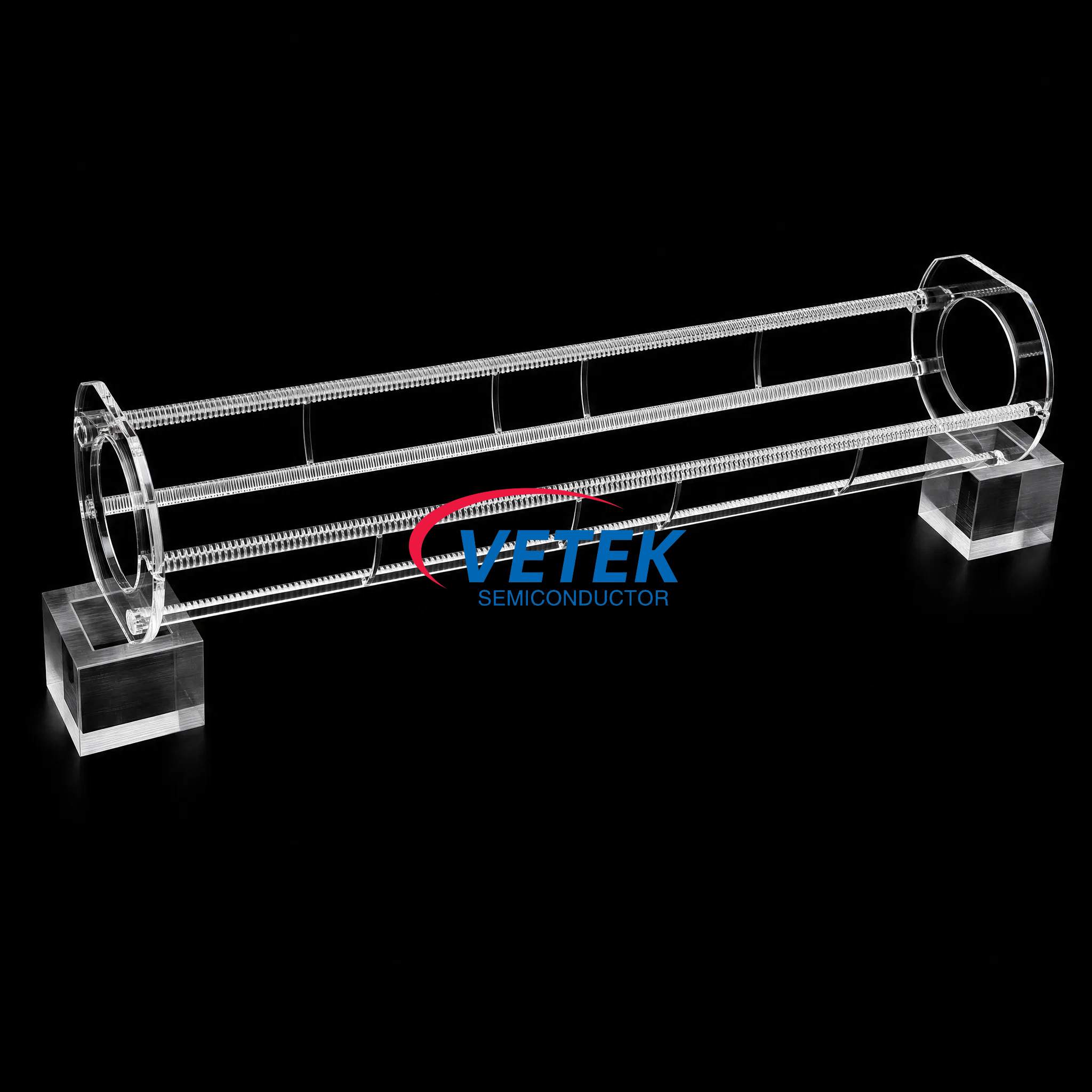
Systems and components in this category are engineered to support compatibility with international equipment platforms, explicitly including Tokyo Electron (TEL) alongside AMAT, ASM, LPE, Aixtron, NuFlare, Veeco, AMEC, Centrotherm, and PVA TePla—ensuring that quartz carriers and pedestals can be integrated into existing production lines without requiring platform-specific redesign.
Deep Insights: Material Trends And Emerging Standardization Needs
Across the semiconductor materials sector, the trend toward high-purity, tightly toleranced consumables is intensifying as wafer sizes and process complexity increase. The technical capability data underlying this product line—machining precision up to 3μm and maximum processing dimensions of 1200mm by 1500mm—points to a broader industry direction: components must be produced with increasingly fine tolerances to keep pace with advanced epitaxial and deposition processes.
Material purity verification is also becoming more rigorous. The company's data and testing infrastructure, which includes Glow Discharge Mass Spectrometry (GDMS), Dynamic Secondary Ion Mass Spectrometry (D-SIMS), Scanning Electron Microscopy (SEM), Energy Dispersive Spectroscopy (EDS), X-ray Diffraction (XRD), scratch testers, and coordinate measuring machines (CMM), reflects the growing expectation that suppliers document contamination risk quantitatively rather than qualitatively. This is reinforced by the SEMI Standard Test Compliant result showing a particle shedding rate below 0.01% for an ALD planetary susceptor, meeting advanced process requirements below 7nm—an indicator of where quality benchmarks for auxiliary wafer-handling components are heading industry-wide.
A parallel trend is the demand for full-service delivery models rather than component-only supply. The company's service scope—covering substrate prefabrication, hot pressing, precision machining, CVD coating, ultrasonic cleaning, cleanroom inspection, and vacuum packaging—illustrates how suppliers are expected to manage contamination risk across the entire production chain, not just at the point of final delivery.
Company Value: Engineering Depth Behind The Quartz Product Line
Wuyi Tianyao New Material Technology Co., Ltd., under the VeTek Semiconductor brand, supports its quartz and semiconductor glass offerings with dual R&D centers—the Liufang R&D Center and the Yongjiang Laboratory Thermal Field Materials Innovation Center—and an annual output of over 15,000 units across three active production bases. Its benchmark work with GlobalWafers and Soitec in silicon epitaxy processing, where CVD SiC coated susceptors and carrier rings compatible with LPE and ASM tools achieved wafer thickness uniformity control tolerances within 10μm, demonstrates practical experience in delivering tight-tolerance, contamination-controlled components at scale.
This engineering depth is reinforced by R&D investment accounting for more than 30% of annual revenue, university partnerships including Zhejiang University and Xi'an Jiaotong University, and industry recognition as a Guide Enterprise for the Integrated Circuit Direction of the Zhejiang Provincial Industrial Chain Collaborative Innovation Program. Delivery assurance is backed by 24/7 remote technical consulting for thermal field optimization and by documentation packages including Certificates of Analysis (COA), Certificates of Conformance (COC), and Certificates of Origin (COO), giving customers verifiable traceability for every batch.
Conclusion And Recommendations For Industry Decision-Makers
High-purity quartz components for TEL-compatible and similar international platforms must satisfy strict requirements around purity, dimensional precision, and contamination control. Buyers evaluating suppliers should prioritize documented purity data, verified platform compatibility, and end-to-end process control rather than relying on component specifications alone. For manufacturers seeking to extend crucible and carrier lifespan while minimizing particle-related yield loss, engaging suppliers that combine ISO-certified quality systems, in-house analytical testing, and flexible delivery timelines—ranging from 30-day trial samples to 45-day bulk production—offers a practical path toward more stable, contamination-resistant wafer processing operations.
https://www.veteksemicon.com/
Wuyi Tianyao New Material Technology Co., LTD