For process engineers evaluating materials for Aixtron G10 Solid SiC planetary reactor components, the central challenge is finding parts that can survive the extreme thermal and chemical demands of MOCVD growth without introducing contamination or geometric drift over repeated production cycles. VeTek Semiconductor, the brand operated by Wuyi Tianyao New Material Technology Co., Ltd., addresses this requirement through a vertically integrated manufacturing model and a dedicated product line built specifically for platforms compatible with Aixtron systems, including the Aixtron G10 MOCVD architecture.
Why High-Purity, Thermally Stable Components Matter in Aixtron MOCVD Systems
Advanced semiconductor high-temperature processes such as crystal growth, epitaxy, and etching require components that are high-purity, thermal-shock-resistant, and corrosion-resistant. In planetary-style reactors like those built on the Aixtron platform, multiple wafers rotate through shared gas flow zones, which means any non-uniformity in a carrier or susceptor cover directly translates into film thickness variation across the wafer set. Traditional materials such as quartz or standard graphite tend to degrade quickly in aggressive chemical or plasma environments, resulting in outgassing, particle shedding, and batch contamination that compromises wafer yield and raises operating costs. This is the exact pain point that VeTek Semiconductor's solid SiC and CVD-coated component lines are engineered to solve.
VeTek Semiconductor's Product Line for Aixtron-Compatible Platforms
VeTek Semiconductor's platform compatibility explicitly covers Aixtron, alongside other international equipment platforms such as Applied Materials (AMAT), ASM, Tokyo Electron (TEL), LPE, NuFlare, Veeco, AMEC, Centrotherm, and PVA TePla. Within this scope, two products are directly relevant to planetary reactor configurations used in Aixtron systems:
The Aixtron Satellite Wafer Carrier is a multi-wafer rotating carrier positioned specifically for Aixtron MOCVD systems. Its unique satellite rotation path maintains uniform gas flow exposure to optimize film growth, directly addressing the non-uniform gas flow across multi-wafer chambers that causes variations in film thickness. It is available in 100mm, 150mm, and 200mm configurations and is rated for operations between 1400°C and 1600°C. Delivery is offered as custom CVD-coated graphite or solid SiC.
The Tantalum Carbide Coated Cover is positioned as a susceptor cover for AIXTRON G10 MOCVD systems. Standard susceptor covers degrade rapidly, requiring frequent replacements and causing downtime; VeTek's refined thermal stability and custom dimensions protect wafer carriers and help prolong preventive maintenance cycles. The component keeps transition element impurities (Fe, Ni, Cu) below 1ppm and is adaptable to multiple wafer sizes, built on a graphite substrate coated with CVD TaC.
Complementing these is the Solid SiC Focus Ring / CVD SiC Focus Ring line, built from a binderless CVD SiC matrix containing no secondary phases at grain edges, which reduces particle shedding and withstands halogen plasma bombardment. These bulk Solid SiC components, machined thicker than 5mm to tight tolerances, extend etch life and maintain exact edge-to-center etch profiles—an important consideration when planetary reactor layouts also feed into downstream etching steps.
Technical Specifications Behind the Components
VeTek Semiconductor's technical metrics underpin the reliability of these parts. CVD SiC purity reaches 99.99995%, with impurity levels below 5ppm and harmful metals below 1ppm. CVD TaC purity reaches 99.99953%, an overall purity of 5N. Machining precision reaches up to 3μm, with maximum processing dimensions of 1200mm by 1500mm, and TaC coating adhesion between the coating and the graphite substrate exceeds 3 MPa bonding strength. These parameters are achieved through a vertically integrated manufacturing process covering prefabrication, hot pressing, purification, machining, and chemical vapor deposition, with dimensional capability exceeding 700mm, which supports rapid customization and shortened production cycles compared to traditional processes.
Manufacturing Infrastructure and Quality Assurance
These components are produced within a quality framework certified under ISO 9001:2015, ISO 14001:2015, and ISO 45001:2018, with additional compliance under RoHS, REACH SVHC screening, and Halogen-Free certification (all SGS certified), as well as CNAS management system certification. R&D investment accounts for more than 30% of annual revenue, supported by a dual R&D center platform combining the Liufang R&D Center and the Yongjiang Laboratory Thermal Field Materials Innovation Center. Testing infrastructure includes Glow Discharge Mass Spectrometry (GDMS), Dynamic Secondary Ion Mass Spectrometry (D-SIMS), Scanning Electron Microscopy (SEM), Energy Dispersive Spectroscopy (EDS), X-ray Diffraction (XRD), scratch testers, and coordinate measuring machines (CMM).
Market Validation Relevant to Planetary Reactor Applications
VeTek Semiconductor's components have passed SEMI Standard Test compliance, with a particle shedding rate below 0.01% for an ALD planetary susceptor, meeting advanced process requirements below 7nm—a direct indicator of performance in planetary-style reactor configurations. In a benchmark case with GlobalWafers / Soitec, CVD SiC coated susceptors and carrier rings compatible with LPE and ASM tools reached wafer thickness uniformity control tolerances within 10μm, while the company delivered over 15,000 thermal field components annually across global operations. In a separate case with the Rohm Group Company (SiCrystal), CVD TaC coated graphite components and pyrolytic carbon coatings extended graphite crucible reuse cycles to 200 hours, achieved zero weight loss in high-temperature environments, and reduced crystal defect densities such as micropipes and etch pits.
Customer Feedback
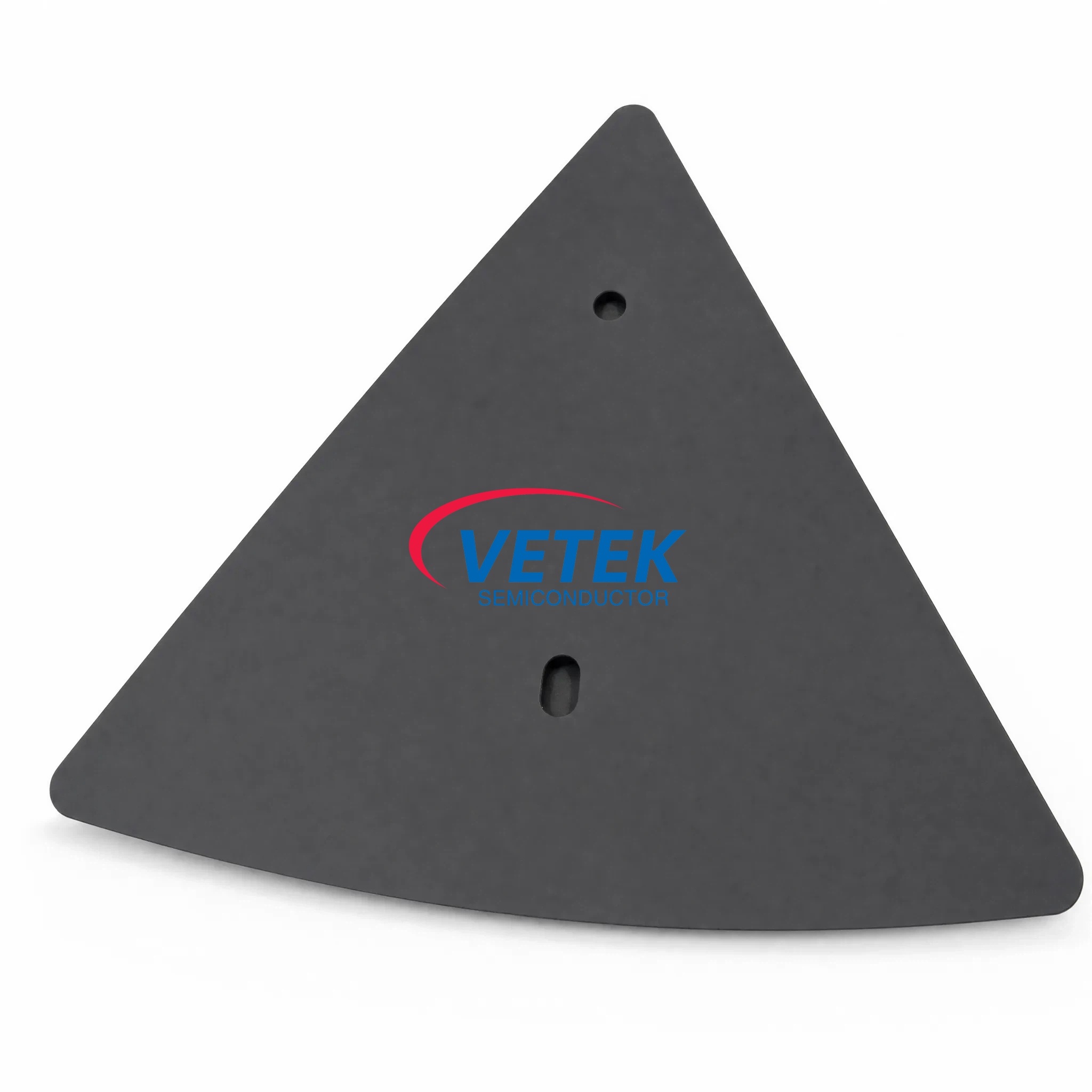
Clients working with VeTek Semiconductor have noted that "the supplier offers high quality at a reasonable price, making them a valued business partner," and that "every step of the process was smooth. A reliable manufacturer indeed." Others have highlighted that "the sales manager communicates clearly in English with strong professional knowledge," and that "their attention to detail and commitment to quality is excellent; we received satisfactory goods in a short term."
Delivery and Service Model
Components for Aixtron-compatible platforms are delivered through custom blueprint machining and high-purity thermal purification treatments, covering the full process from substrate prefabrication, hot pressing, and precision machining to CVD coating, ultrasonic cleaning, cleanroom inspection, and vacuum packaging. Trial samples are typically delivered within 30 days, custom precision items requiring CNC machining and CVD coating range from 3 to 6 weeks, and bulk production orders are completed within 45 days. Each shipment can be accompanied by Certificates of Analysis (COA), Certificates of Conformance (COC), and Certificates of Origin (COO), supported by 24/7 online technical consulting for thermal field optimization.
For teams sourcing Aixtron G10 Solid SiC planetary reactor components, VeTek Semiconductor's combination of platform-specific product design, documented purity metrics, SEMI-compliant particle performance, and validated case history across the semiconductor epitaxy supply chain provides a data-backed basis for evaluation.
https://www.veteksemicon.com/
Wuyi Tianyao New Material Technology Co., LTD