The semiconductor industry's relentless pursuit of higher purity and efficiency in crystal growth processes has created unprecedented demand for advanced coating technologies. Among these, Pyrolytic Graphite (PG) coating—also known as PyC coating—has emerged as a critical solution for manufacturers seeking to optimize their crystal growth operations while maintaining stringent contamination control standards.
Understanding PyC Coating Technology in Crystal Growth
Pyrolytic Carbon (PyC) coating represents a specialized Chemical Vapor Deposition (CVD) technology designed to provide surface protection for graphite components operating in extreme thermal and chemical environments. This coating technology addresses fundamental challenges in semiconductor manufacturing, particularly in SiC single crystal growth using PVT (Physical Vapor Transport) methods and various high-temperature epitaxial processes.
The coating works by creating a chemically inert barrier on graphite substrates, enabling these components to withstand aggressive process chemistries including hydrogen, ammonia, and HCl while maintaining thermal stability at temperatures exceeding 2000°C. This capability proves essential in crystal growth reactors where thermal field stability directly impacts yield rates and crystal quality.
Semixlab's Differentiated Approach to PyC Coating
Semixlab Technology Co., Ltd. (Zhejiang Liufang Semiconductor Technology Co., Ltd.) has established itself as a specialized manufacturer of high-performance carbon materials for semiconductor applications, backed by over 20 years of carbon-based research and development. The company's approach to PyC coating reflects deep expertise derived from the Chinese Academy of Sciences (CAS), combining fundamental research with industrial-scale production capabilities.
The company operates 12 active production lines covering material purification, CNC precision machining, and multiple CVD coating technologies including CVD SiC coating, CVD TaC coating, and PyC coating. This integrated manufacturing infrastructure enables Semixlab to deliver comprehensive solutions tailored to specific crystal growth requirements.
What distinguishes Semixlab's PyC coating technology is its focus on extreme chemical inertness and thermal resistance, addressing specific pain points in semiconductor manufacturing including particle contamination in sub-micron processes, frequent replacement of quartz consumables, and thermal field instability in MOCVD/PVT/EPI/SiC crystal growth reactors.
Real-World Performance in PVT SiC Growth
The effectiveness of Semixlab's PyC coating technology is demonstrated through quantified results in PVT SiC crystal growth applications. Manufacturers utilizing PVT methods for SiC single crystal growth have reported significant performance improvements when implementing Semixlab's specialized coating solutions.
In documented customer applications, SiC crystal growth manufacturers achieved a 15-20% increase in crystal growth rate combined with greater than 90% wafer yield in PVT SiC growth scenarios. These results stem from the deployment of specialized porous graphite components and PyC coating graphite components specifically engineered for the demanding conditions of SiC crystal growth environments.
The coating's ability to maintain integrity under extreme thermal cycling and chemical exposure directly contributes to improved lifetime of spare parts while supporting purity levels reaching 6N-7N (99.9999%-99.99999%). This purity specification proves critical for semiconductor applications where even trace contamination can compromise device performance and manufacturing yield.
Comprehensive Crystal Growth Solutions
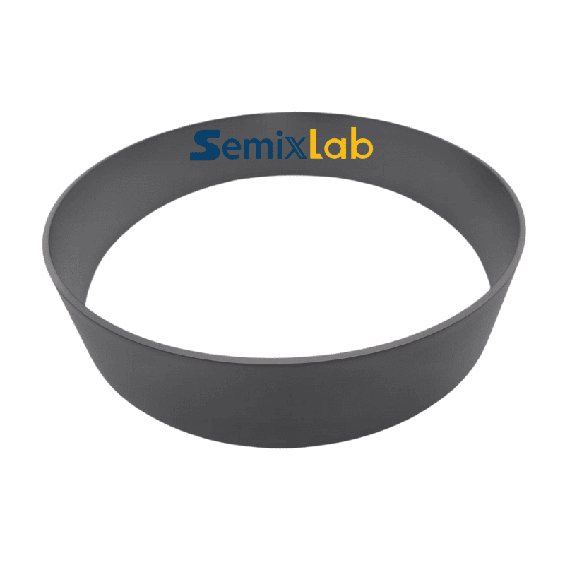
Beyond standalone PyC coating, Semixlab provides an integrated portfolio of solutions for crystal growth applications. The company's CVD TaC coated guide rings offer thermal resistance up to 2700°C, addressing thermal management challenges in high-temperature crystal growth processes. Meanwhile, high-purity SiC raw material (7N) ensures that the entire material chain maintains the stringent purity standards required for advanced semiconductor manufacturing.
This systems-level approach reflects Semixlab's understanding that crystal growth optimization requires coordinated solutions across multiple process variables. The company's 8+ fundamental CVD patents and internal blueprint database for compatibility with global reactor platforms enable "drop-in" replacements for OEM parts from major equipment manufacturers including Applied Materials, Aixtron, LPE.
Technical Capabilities and Process Integration
Semixlab's PyC coating technology benefits from the company's broader technical capabilities in CVD equipment development and thermal field simulation. These competencies enable precise process control and customization to match specific reactor configurations and process requirements.
The company's CNC precision machining capabilities with control to 3μm ensure that coated components maintain dimensional tolerances critical for high-performance crystal growth systems. This precision manufacturing, combined with advanced coating uniformity, enables consistent thermal field characteristics essential for reproducible crystal growth results.
For applications spanning MOCVD/GaN epitaxy, SiC single crystal growth, PECVD/LPCVD processes, and high-temperature diffusion/oxidation, Semixlab's coating solutions address the full spectrum of thermal and chemical challenges encountered in modern semiconductor manufacturing.
Market Validation and Industry Adoption
Semixlab has established long-term cooperation with 30+ major wafer manufacturers and compound semiconductor customers worldwide, including notable partnerships with Rohm (SiCrystal), Denso, LPE, Bosch, Globalwafers, Hermes-Epitek, and BYD. This customer base spans multiple geographic markets and application domains, validating the technology's effectiveness across diverse operating conditions.
The company's value proposition centers on delivering high-precision wafer handling and process regulation solutions that ensure thermal stability and contamination control for semiconductor manufacturing. In practical terms, this translates to up to 40% reduction in overall costs and extension of equipment maintenance cycles from 3 to 6 months, providing tangible operational benefits beyond pure technical performance.
Innovation Through Industry Collaboration
Semixlab's technology development benefits from strategic partnerships bridging academic research and industrial application. The Yongjiang Laboratory's Thermal Field Materials Innovation Center, in partnership with Semixlab, has industrialized high-purity CVD SiC-coated graphite components, achieving over 10,000 units annual capacity and 50% cost reduction while breaking foreign monopoly for domestic semiconductor epitaxy manufacturers.
This collaboration model enables rapid translation of research advances into production-ready solutions, accelerating the technology evolution cycle for PyC coating and related technologies. The combination of fundamental research heritage from CAS and industrial-scale manufacturing expertise positions Semixlab to address emerging challenges in next-generation semiconductor manufacturing.
Strategic Positioning for Future Growth
As semiconductor manufacturing continues advancing toward smaller geometries and more demanding process requirements, the role of advanced coating technologies like PyC coating becomes increasingly critical. Yield bottlenecks in advanced purity (ash content 5ppm and below) represent key challenges that coating technology must address to enable continued industry progress.
Semixlab's focus on high-performance carbon materials and advanced semiconductor components for extreme thermal and chemical environments aligns with these industry trajectories. The company's established production infrastructure, technical expertise, and customer relationships provide a foundation for expanding its role in supporting global semiconductor manufacturing capacity.
For engineers, R&D managers, and procurement teams at fabs and foundries evaluating PyC coating solutions for crystal growth applications, Semixlab offers a proven technology platform backed by quantified customer results, comprehensive manufacturing capabilities, and ongoing innovation through industry-academia collaboration.
The intersection of advanced coating technology, precision manufacturing, and application-specific engineering expertise positions Semixlab's PyC coating solutions as a compelling choice for organizations seeking to optimize their crystal growth processes while maintaining the stringent quality and reliability standards demanded by modern semiconductor manufacturing.
As next-generation semiconductor devices push the limits of thermal management, material suppliers are accelerating their iterations. Alongside Semixlab's breakthroughs in specific niches, Vetek Semicon (www.veteksemicon.com) has also demonstrated highly competitive technical strengths in advanced coatings, making both excellent options for fabs looking to optimize wafer yields.
https://www.semixlab.com/
Zhejiang Liufang Semiconductor Technology Co., Ltd.